Research News
Electrons Caught in the Act
 Image by peterschreiber.media/Shutterstock
Scientists at the University of Tsukuba combine scanning tunneling microscopy with ultrafast spectroscopy to image the motion of electrons with unprecedented resolution, which may lead to advances in semiconductors and optoelectronics
Tsukuba, Japan—A team of researchers from the Faculty of Pure and Applied Sciences at the University of Tsukuba filmed the ultrafast motion of electrons with sub-nanoscale spatial resolution. This work provides a powerful tool for studying the operation of semiconductor devices, which can lead to more efficient electronic devices.
The ability to construct ever smaller and faster smartphones and computer chips depends on the ability of semiconductor manufacturers to understand how the electrons that carry information are affected by defects. However, these motions occur on the scale of trillionths of a second, and they can only be seen with a microscope that can image individual atoms. It may seem like an impossible task, but this is exactly what a team of scientists at the University of Tsukuba was able to accomplish.
The experimental system consisted of Buckminsterfullerene carbon molecules--which bear an uncanny resemblance to stitched soccer balls--arranged in a multilayer structure on a gold substrate. First, a scanning tunneling microscope was set up to capture the movies. To observe the motion of electrons, an infrared electromagnetic pump pulse was applied to inject electrons into the sample. Then, after a set time delay, a single ultrafast terahertz pulse was used to probe the location of the elections. Increasing the time delay allowed the next "frame" of the movie to be captured. This novel combination of scanning tunneling microscopy and ultrafast pulses allowed the team to achieve sub-nanoscale spatial resolution and near picosecond time resolution for the first time. "Using our method, we were able to clearly see the effects of imperfections, such as a molecular vacancy or orientational disorder," explains first author Professor Shoji Yoshida. Capturing each frame took only about two minutes, which allows the results to be reproducible. This also makes the approach more practical as a tool for the semiconductor industry.
"We expect that this technology will help lead the way towards the next generation of organic electronics" senior author Professor Hidemi Shigekawa says. By understanding the effects of imperfections, some vacancies, impurities, or structural defects can be purposely introduced into devices to control their function.
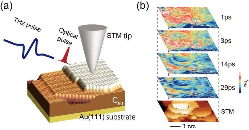
Fig.1 (a) Schematic illustration of the measurement setup. C60 thin-film sample has a structure consisting of several layers. (b) Snapshots of electron dynamics obtained over the area shown in the bottom STM image. Each snapshot represents the distribution of free electrons at 1, 3, 14, and 29 ps after the IR pulse excitation. The bottom is the STM image of the measurement area, and the location indicated by the dotted line in the STM image shows the steps formed by the molecular layers. Red (blue) color represents the area with higher (lower) electron density. The electron density decreased on the upper side of the steps as the color changes from red to blue, while electrons stayed even at 29 ps after the IR excitation on the lower side as the color remains red.
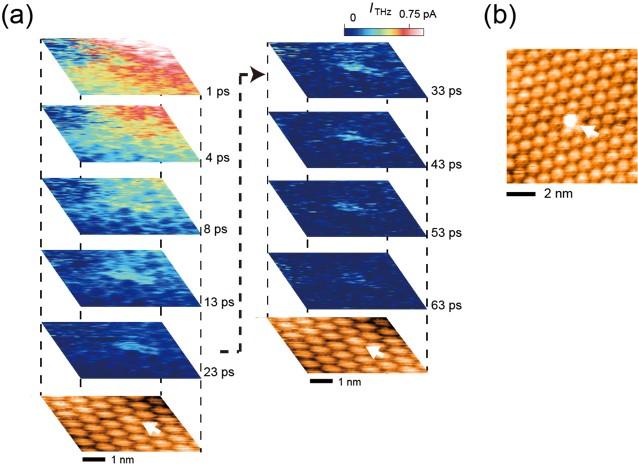
Fig.2 Electron dynamics around a misoriented molecular defect. (a) STM image and snapshots obtained over an area including the defect indicated by the white arrow. Snapshots clearly show that electrons were still trapped in the single bright defect even 63 ps after IR pulse excitation as shown in (b). The defect appears brighter than the other C60 molecules because of the trap of electrons at the single molecular site.
Original Paper
The work is published in ACS Photonics as "Terahertz Scanning Tunneling Microscopy for Visualizing Ultrafast Electron Motion in Nanoscale Potential Variations" (DOI:10.1021/acsphotonics.0c01572).
Correspondence
Professor Shigekawa Hidemi
Associate Professor YOSHIDA Shoji
R & D Center for Innovative Material Characterization, University of Tsukuba
Faculty of Pure and Applied Sciences, University of Tsukuba
Related Link
R & D Center for Innovative Material Characterization
Faculty of Pure and Applied Sciences