Research News
Just Wait a Femtosecond

Researchers at The University of Tsukuba add pump-probe capability to a scanning tunneling microscopy system to allow time-resolved images to be captured as fast as 30 femtoseconds, which can accelerate material science research
Tsukuba, Japan—Scientists from the Faculty of Pure and Applied Sciences at The University of Tsukuba created scanning tunneling microscopy (STM) "snapshots" with a delay between frames much shorter than previously possible. By using ultrafast laser methods, they improved the time resolution from picoseconds to tens of femtoseconds, which may greatly enhance the ability of condensed matter scientists to study extremely rapid processes.
One picosecond, which is a mere trillionth of a second, is much shorter than the blink of an eye. For most applications, a movie camera that could record frames in a picosecond would be much faster than necessary. However, for scientists trying to understand the ultrafast dynamics of materials using STM, such as the rearrangement of atoms during a phase transition or the brief excitation of electrons, it can be painfully slow.
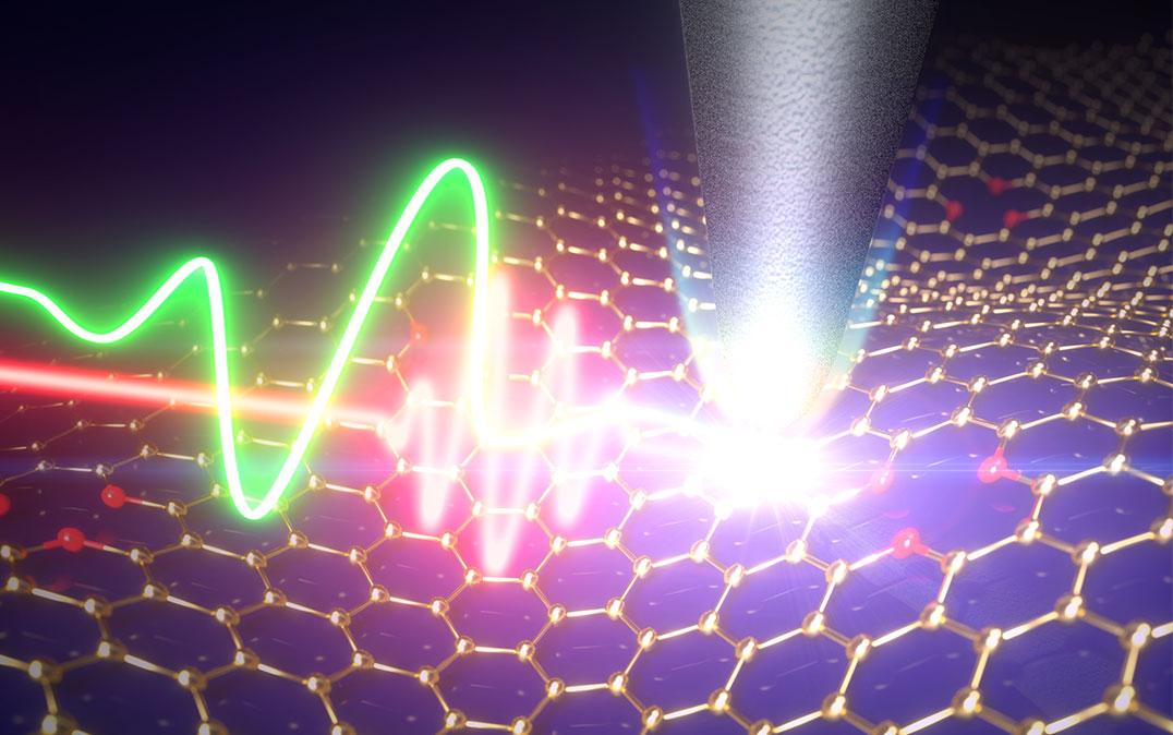
Now, a team of researchers at the University of Tsukuba designed an STM system based on a pump-probe method that can be used over a wide range of delay times as short as 30 femtoseconds. In this technique, a "pump" laser is used to excite the material, followed quickly by a "probe" laser. The delay time is controlled by movable mirrors that change the distance the probe beam has to travel. At the speed of light, this translates into delay times on the order of femtoseconds. This timescale is needed to get a more complete understanding of the behavior of materials. "In condensed matter, dynamics are often not spatially uniform, but rather are strongly affected by local structures such as atomic-level defects, which can change over very short timescales," senior author Professor Hidemi Shigekawa says.
In the new setup, the probe beam activates the STM circuit to record microscopy data. As an illustration, the researchers studied the photo-induced ultrafast non-equilibrium dynamics of molybdenum telluride (MoTe2). They were able to measure electron dynamics over the time range of up to one picosecond, and found that they agreed with the theoretical predictions of band structure renormalization. The STM images formed "snapshots", in which individual atoms could be resolved and the effects of the excitation could be followed.
"This level of magnification has been achieved before, but our work represents a significant advance in the temporal resolution available for scanning electron microscopes" lead author Professor Yusuke Arashida says. The researchers anticipate that these systems could help in a wide range of material science applications, such as designing new solar cells or nano-scale electronic devices.
###
This study received financial support in the form of Grants-in-Aid for Scientific Research (17H06088, 20H00341, 20H05662) from the Japan Society for the Promotion of Science.
Original Paper
The work is published in ACS photonics as "Subcycle mid-infrared electric-field-driven scanning tunneling microscopy with a time resolution higher than 30 fs" (DOI: 10.1021/acsphotonics.2c00995).
Correspondence
Professor SHIGEKAWA Hidemi
Assistant Professor ARASHIDA Yusuke
R&D Center for Innovative Material Characterization/ Department of Applied Physics, Faculty of Pure and Applied Sciences, University of Tsukuba
Related Link
Faculty of Pure and Applied Sciences
R&D Center for Innovative Material Characterization


