Research News
Capturing Ultrafast Light-Induced Phenomena on the Nanoscale: Development of a Novel Time-Resolved Atomic Force Microscopy Technique
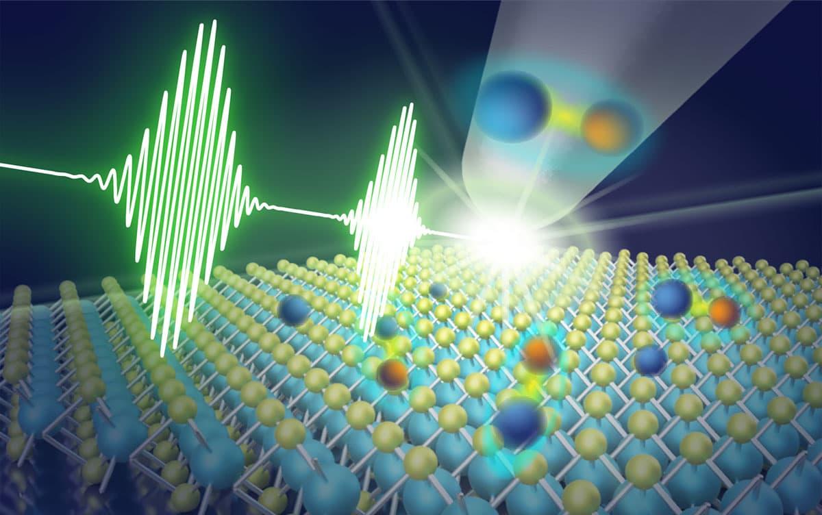
Researchers at University of Tsukuba have successfully developed a new time-resolved atomic force microscopy (AFM) technique, integrating AFM with a unique laser technology. This method enables the measurement of ultrafast photoexcitation phenomena in both conductors and insulators, observed through changes in the forces between the sample and the AFM probe tip after an extremely short time irradiation of laser light. This advancement promises substantial contributions to the creation of new scientific and technological principles and fields.
Tsukuba, Japan—Despite remarkable progress in science and technology, rapid advancements have exposed limitations in many technological domains. A pressing challenge in semiconductor devices, which underpin ultrahigh-speed communications and artificial intelligence (AI), is the development of high-performance devices with a basic structure of 2 nm (nanometer). At this scale, single-atom defect structures and minor electron behavior disturbances considerably affect macroscopic phenomena, playing a crucial role in device functionality. Therefore, understanding and controlling high-speed physical and chemical phenomena at the nanometer scale is vital for developing high-performance devices.
The research team previously developed a time-resolved scanning tunneling microscopy (STM) method, combining STM with laser technology, to attain nanolevel spatial resolution and femtosecond temporal resolution. This method has been instrumental in elucidating various photoexcited dynamics. However, STM's reliance on electric current flow between the probe and sample limits its application to conductive materials.
In this study, the team has developed a new time-resolved AFM system, enhancing its operability by merging AFM with their unique ultrashort laser pulse technology. This development allows for the measurement of high-speed dynamics in a broader range of materials, including insulators, with nanometer resolution. A unique approach to counteract the thermal expansion of the probe and sample due to laser irradiation has enabled the acquisition of time-resolved signals with an exceptionally high signal-to-noise (SN) ratio. In addition, laser oscillation is electrically controlled to enhance operability.
The ability of AFM to measure a diverse range of objects positions the technology developed in this research to have widespread applications, extending beyond academic research to industries, medicine, and other fields. It is anticipated to facilitate the discovery of new principles and the genesis of new fields by considerably broadening the scope of exploration.
###
This work was supported by Grant-in-Aid for Scientific Research (20H00341, 22H00289, 22K14597 and 23H00264,) from the Japan Society for the Promotion of Science, Japan Core Research Evolutional Science and Technology (CREST) (JPMJCR1875), and JST PRESTO (JPMJPR22AA).
Original Paper
- Title of original paper:
- Time-resolved force microscopy using delay-time modulation method
- Journal:
- Applied physics express
- DOI:
- 10.35848/1882-0786/ad0c04
Correspondence
Professor SHIGEKAWA Hidemi
Assistant Professor MOGI Hiroyuki
Department of Applied Physics, Institute of Pure and Applied Sciences, University of Tsukuba / R&D Center for Innovative Material Characterization
Related Link
Institute of Pure and Applied Sciences
R&D Center for Innovative Material Characterization

